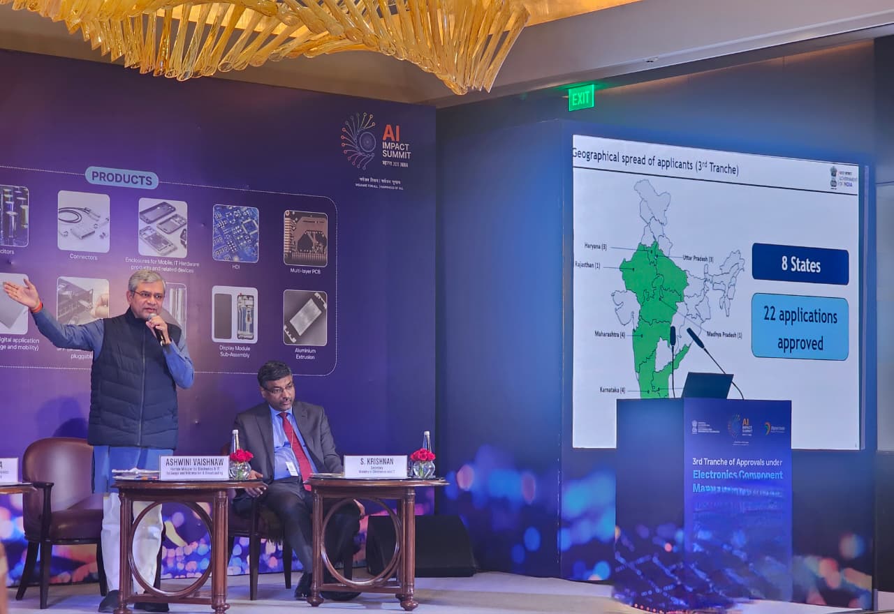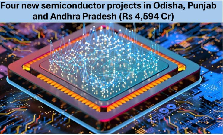
In a significant step toward establishing India as a global hub for semiconductor manufacturing, the Union Cabinet, chaired by Prime Minister Narendra Modi, approved four new semiconductor projects under the India Semiconductor Mission (ISM) on August 12, 2025. These projects, with a cumulative investment of approximately Rs. 4,600 crore, will be established in Odisha, Punjab, and Andhra Pradesh, further strengthening the nation’s burgeoning semiconductor ecosystem.
The approvals bring the total number of sanctioned projects under the ISM to ten, with a combined investment of around Rs. 1.60 lakh crore across six states, positioning India as a key player in the global semiconductor supply chain.
The four newly approved projects, spearheaded by SiCSem Private Limited, Continental Device India Private Limited (CDIL), 3D Glass Solutions Inc., and Advanced System in Package (ASIP) Technologies, are expected to generate direct employment for 2,034 skilled professionals while catalyzing the electronics manufacturing ecosystem, leading to thousands of indirect job opportunities.
These initiatives align with India’s vision of becoming self-reliant, or Atmanirbhar Bharat, by addressing the growing demand for semiconductors in critical sectors such as telecommunications, automotive, data centers, consumer electronics, and industrial electronics.
In Odisha, SiCSem Private Limited, in collaboration with Clas-SiC Wafer Fab Ltd. of the UK, will establish the country’s first commercial compound semiconductor fabrication facility in Info Valley, Bhubaneswar. This integrated facility will focus on manufacturing Silicon Carbide (SiC) devices, which are critical for high-power applications.
With an annual production capacity of 60,000 wafers and a packaging capacity of 96 million units, the facility will cater to diverse applications, including missiles, defense equipment, electric vehicles (EVs), railway systems, fast chargers, data center racks, consumer appliances, and solar power inverters. The establishment of this compound semiconductor fab marks a milestone in India’s journey toward advanced semiconductor manufacturing.
Also in Odisha, 3D Glass Solutions Inc. (3DGS) will set up a vertically integrated advanced packaging and embedded glass substrate unit in Info Valley, Bhubaneswar. This facility will introduce the world’s most advanced packaging technology to India, revolutionizing semiconductor efficiency.
The unit will produce glass interposers with passives, silicon bridges, and 3D Heterogeneous Integration (3DHI) modules, with an annual capacity of approximately 69,600 glass panel substrates, 50 million assembled units, and 13,200 3DHI modules. These products will find applications in defense, high-performance computing, artificial intelligence, radio frequency (RF), automotive, photonics, and co-packaged optics, significantly enhancing India’s capabilities in cutting-edge technologies.
In Andhra Pradesh, Advanced System in Package Technologies (ASIP), in collaboration with APACT Co. Ltd. of South Korea, will establish a semiconductor manufacturing unit with an annual capacity of 96 million units.
The facility will produce components for mobile phones, set-top boxes, automotive applications, and other electronic products, further diversifying India’s semiconductor manufacturing portfolio and supporting the growing demand for consumer electronics.
In Punjab, Continental Device India Private Limited (CDIL) will expand its existing discrete semiconductor manufacturing facility in Mohali. This brownfield expansion will focus on producing high-power discrete semiconductor devices, including MOSFETs, IGBTs, Schottky Bypass Diodes, and transistors in both Silicon and Silicon Carbide.
With an annual capacity of 158.38 million units, the facility will serve applications in automotive electronics, including EVs and their charging infrastructure, renewable energy systems, power conversion, industrial applications, and communication infrastructure. This expansion underscores India’s commitment to strengthening its domestic manufacturing capabilities for critical electronic components.
These projects complement India’s growing expertise in chip design, supported by the government’s initiatives to provide design infrastructure to 278 academic institutions and 72 startups. Over 60,000 students have already benefited from talent development programs under the ISM, fostering a skilled workforce to drive the semiconductor industry forward.
The approved projects, including the nation’s first commercial compound fab and an advanced glass-based substrate packaging unit, are poised to enhance India’s technological self-reliance and global competitiveness.
With these developments, India is not only building a robust semiconductor ecosystem but also positioning itself as a vital contributor to the global supply chain.
The projects are expected to meet the rising demand for semiconductors across industries, reduce import dependency, and create a ripple effect of economic growth through job creation and technological innovation. As the India Semiconductor Mission gains momentum, the nation is steadily advancing toward its goal of becoming a self-reliant powerhouse in the global electronics market.